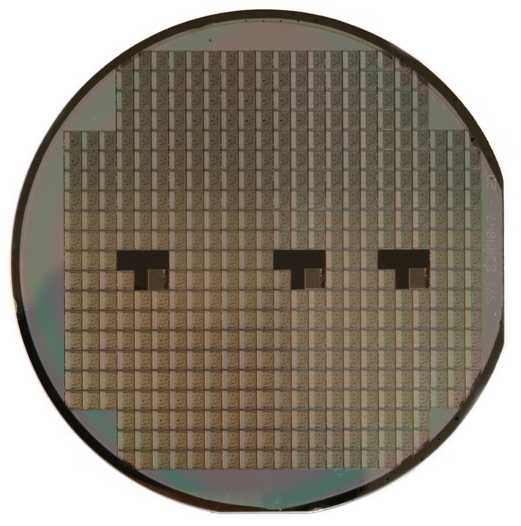
Researchers at Caltech have built optical pathways on silicon chips that lose very little light — approaching the efficiency of optical fibre, and performing far better than existing on-chip technology at visible wavelengths. The work was reported on 17 August.
Advertisement — ad space reserved
What a waveguide is, and why loss matters
A waveguide is a channel that carries light, in the same way a wire carries electricity. On a chip it is a strip of transparent material only a fraction of the width of a human hair, laid down alongside the other components.
Light travelling along it does not arrive intact. Some is absorbed by the material and some scatters off imperfections in the walls of the channel — and at the scale of a chip, a surface roughness of a few atoms is a meaningful imperfection. That is loss, and it accumulates with distance.
Loss sets what is possible. A signal that fades quickly has to be amplified, which costs power and adds noise. In quantum applications, where the point is often a single photon, an absorbed photon is not a weakened signal — it is a lost one. Reducing loss does not merely make existing devices better; it changes which devices can exist at all.
Why visible light is the hard case
Silicon photonics has largely been developed around the infrared wavelengths used by telecommunications, because that is where the money and the fibre networks are. Visible light has been comparatively neglected on-chip, and it is technically harder: shorter wavelengths scatter more off the same imperfection, so a surface that is smooth enough for infrared is not smooth enough for blue or green.
Visible wavelengths are also what a great deal of science and medicine actually needs. Biological imaging, fluorescence microscopy, atomic clocks and many quantum systems based on trapped atoms and ions all operate in the visible range. Making that range work on a manufacturable silicon chip is what would move these systems from optical benches the size of a table onto something that can be produced in quantity.
Advertisement — ad space reserved
What is claimed, and what follows
The claim reported is comparative: performance approaching optical fibre, and a large improvement on existing on-chip options in the visible range. The applications suggested include more powerful chip-scale lasers.
The gap between a laboratory result and a product is where most of this kind of news quietly ends, and it is worth naming the specific hurdles rather than offering a generic caution. A result demonstrated on a small number of devices has to survive manufacturing at volume, where yield and variation between chips decide viability. It has to work when integrated with lasers, detectors and control electronics rather than in isolation. And it has to be compatible with existing semiconductor fabrication processes, because a technique that requires a new kind of factory tends not to be adopted however good it is.
None of that means the result is unimportant. Incremental reductions in optical loss have driven this field for two decades, and the ones that hold up are the reason chip-scale photonics exists at all.
Why to care about a technical result
The honest answer is that most people will never encounter this directly, and the effects arrive indirectly and late. If it holds, the visible consequences are things like portable instruments that currently require a laboratory, more compact quantum hardware, and lower power consumption in the data infrastructure that increasingly moves information as light rather than electricity.
Those are plausible directions rather than promises. The result itself is narrower and more solid: light can be moved further across a silicon chip, at wavelengths we can see, with less of it lost on the way.
Sources
Advertisement — ad space reserved
Leave a Reply